Junctions with low resistance between subcells are essential for realizing high efficiency tandem solar cells. We fabricated pn junctions of a variety of semiconductor materials (Si, GaAs, InGaP) with varied doping concentrations using hybrid approaches (surface activated bonding). Their electrical properties were investigated by I-V measurements.
(Result)
We made pn junctions of semiconductor layers with polarities and doping concentrations shown in Table I. Several of I-V characteristics of fabricated pn junctions are shown Fig. 1. Lower resistances are observed for junctions with more heavily doped layers. The p+-GaAs/n++-Si junction reveals the lowest resistance (0.13 W cm2) among the prepared samples. The power loss and the degradation in conversion efficiency against the effective doping concentration is estimated for the respective pn junctions on the assumption that the short circuit current (JSC) is 44 mA/cm2, or the ideal JSC for two-junction cells with Si bottom cells for air mass 1.5G and one sun illumination (Fig. 2). The power loss hence the degradation in conversion efficiency is reduced by increasing the effective doping concentration. The power loss and the degradation in conversion efficiency for the p+-GaAs/n++-Si junction are as low as 0.063 mW/cm2 and 0.063%, respectively.
Table I. Polarities and carrier concentrations of semiconductor layers
for pn junctions.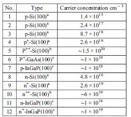 |
||
 |
 |
|
| Fig. 1. I-V characteristics of (a) p+-GaAs/n++-Si, (b) p+-GaAs/n+-Si, (c) p+-Si/n+-Si, (d) p++-Si/n+-InGaP, and (e) p+-Si/n+-InGaP junctions measured at room temperature. | Fig. 2. Power loss and degradation in conversion efficiency against effective doping concentration estimated for two-junction tandem cells with JSC of 22 mA/cm2. | |