It is assumed that narrow-gap/wide-gap semiconductor heterojunctions can be an essential block for simultaneously realizing power devices with high switching speeds and large breakdown voltages. As one possible candidate for such heterojunctions, Si (bandgap of 1.12 eV at room temp.)/SiC (3.26 eV) heterojunctions were fabricated by using direct wafer bonding with the surface-activation process. We investigated the dependence of their electrical properties on the thermal process and found that the electrical properties were improved. The impact of the annealing on the structural properties at Si/SiC interfaces was also examined by TEM observation.
(Result)
I-V characteristics of p+-Si/n--SiC heterojunctions that we fabricated were measured after the annealing at a variety of temperatures. The magnitude of the current for reverse-bias voltages decreased below the measurement limit as the annealing temperature increased up to 1000 deg. Celsius. Simultaneously, humps in the I-V characteristics for foward bias voltages became less marked due to the annealing at higher temperatures.
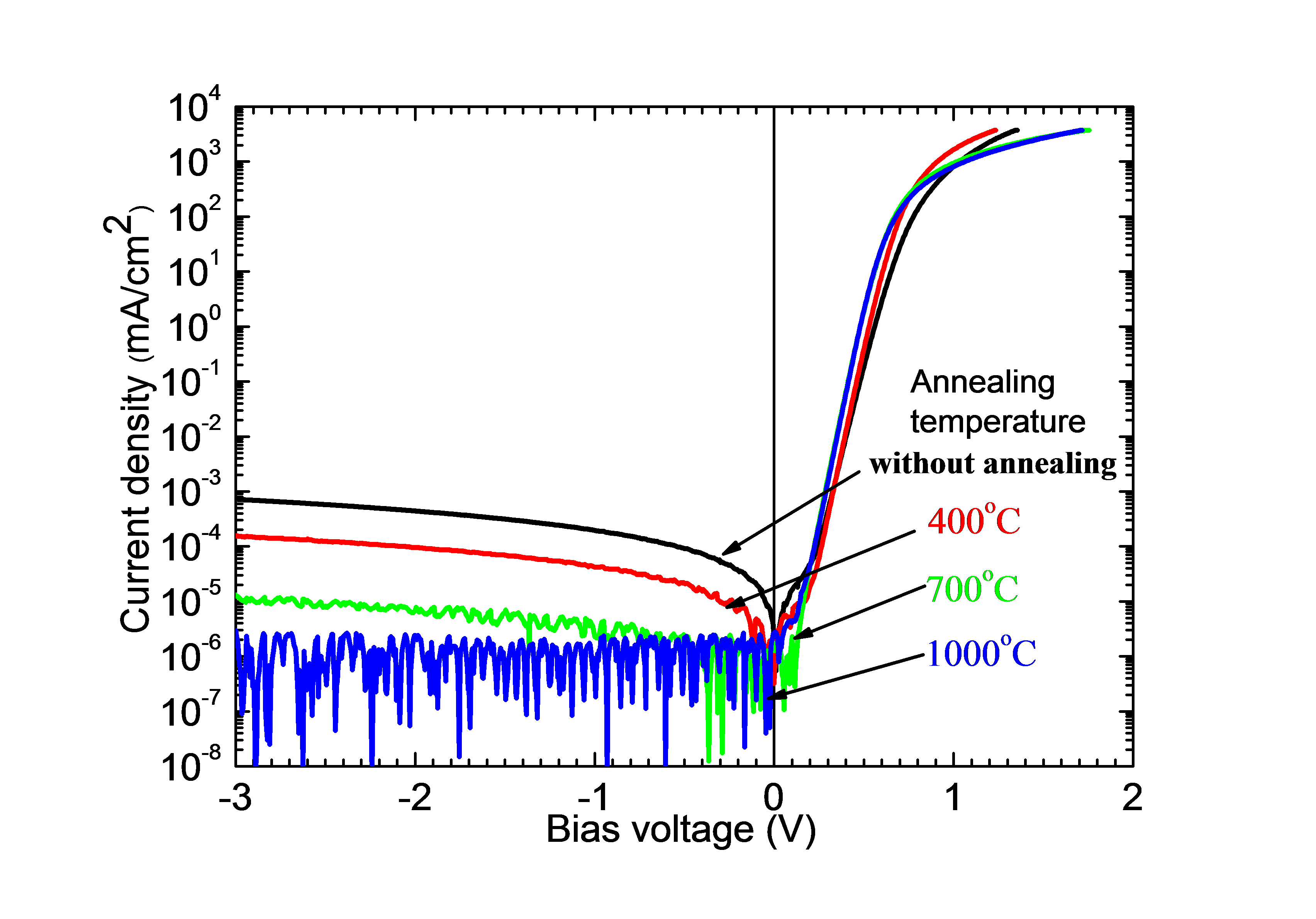 |
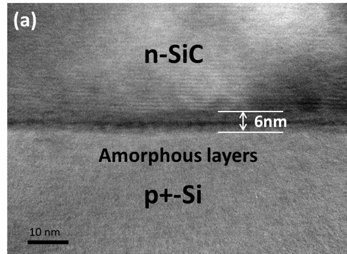
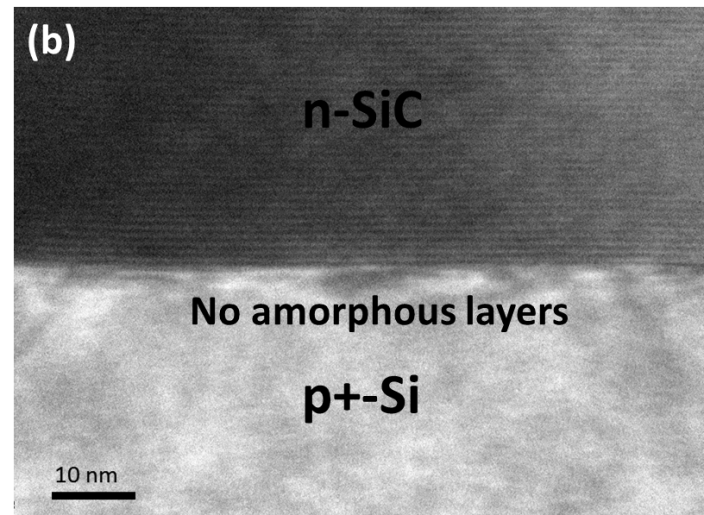
The TEM observation revealed that the amorphous layer that had been formed at the Si/SiC interfaces disappeared after the annealing, which suggests that the amorphous layer was re-crystallized. The structural change at the interface might be related to the improvement of the electrical properties. The details are reported in Appl. Phys. Lett. 104, 161604 (2014).
 |
 |
|
| A TEM image of an Si/SiC junction before annealing. | A TEM image of an Si/SiC junction after annealing at 1000 deg. Celsius. |
(Note) This work was jointly performed with New Japan Radio Co. Ltd.