Heterojunctions composed of III-V compound semiconductors epitaxially-grown on group-IV substrates are attractive elements for innovative photovoltaic devices as well as for advanced electron and photonic devices. We have another approach for fabricating such heterostructures, which is so called “hybrid” approach, or bonding semiconductor layers on substrates. Usage of such hybrid approaches is likely to enable us to achieve heterostructures composed of semiconductor materials with different crystal structures and/or different lattice constants, which is the advantage of the hybrid approaches in comparison with epitaxial-growth-based approaches. Si-on-Si (n-Si/n-Si and p-Si/n-Si) junctions were fabricated by using surface-activated bonding (SAB) of Si substrates and their structural and electrical properties were characterized. Issues associated with the hybrid approach such as electrical properties at interfaces are addressed.
(Result)
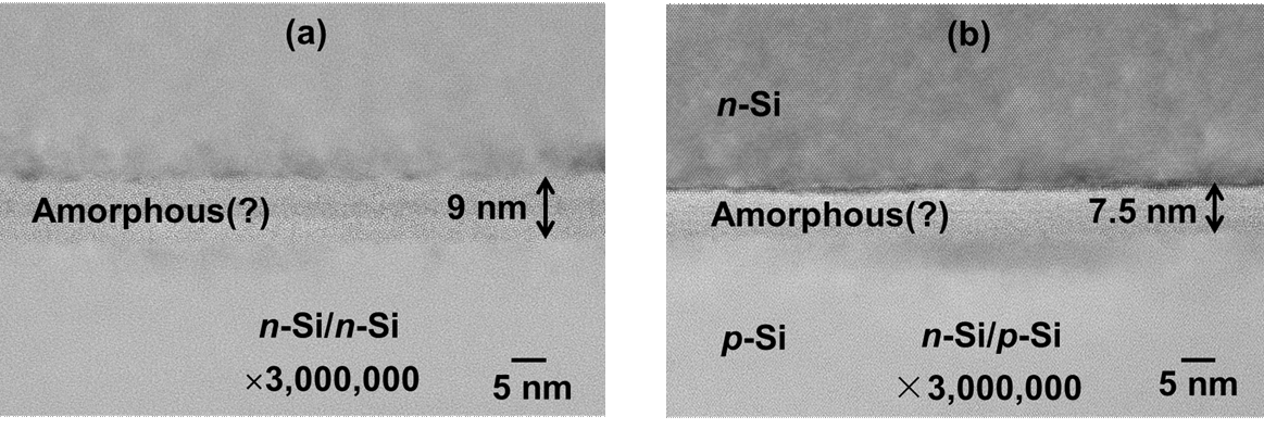
We performed XTEM observation of the interfaces of Si/Si junctions and found that several-nm thick amorphous-like layers were formed at bonding interfaces.
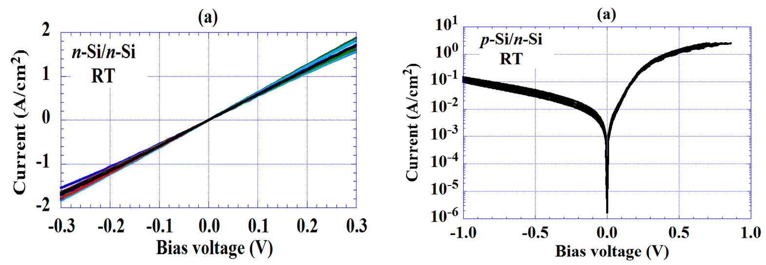
By measuring the current-voltage (I-V) characteristics at room temperature, we found that n-Si/n-Si junctions revealed ohmic features. The p-Si/n-Si junctions showed rectifying properties similarly to conventional pn junctions. These results mean that amorphous-like layers at the interfaces do not cause serious impacts on the electrical properties of junctions at room temperature, which suggests that SAB-based junctions might be applicable for fabricating novel semiconductor devices.
(Note) This work is jointly performed with Prof. Higurashi's group in Univ. of Tokyo.