The single-crystal diamond is the most promising semiconductor as vital part of power devices because ot its excellent material properties such as the largest figure of merit and highest thermal conductivity among the major semiconductors. Although promising pioneering results were reported, the R&D of diamond-based electron devices, however, has not yet been active for the present because the size of single-crystal diamond substrates does not match with facilities for the semiconductor device process. We understand that the direct bonding of single-crystal diamonds to Si substrates could be a solution for this issue. In this work, we applied surface activated bonding (SAB) technologies for fabricating diamond/Si junctions and examined their interface properties.
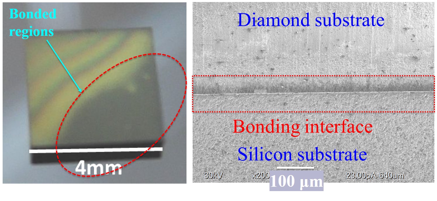 |
| A top view and SEM image of single-crystal diamond/Si junctions. |
(Result)
A 4-mm-by-4-mm single-crystal diamond was bonded to a Si substrate using the SAB without heating. The top view of the junction (above left) showed that a ≈ 40% of the diamond surface was successfully adhered to a Si substrate. We obtained interfaces without cracks as shown in the SEM image (above right).
We also performed TEM and EELS observation of diamond/Si interfaces. A several-ten-nm-thick amorphous-like layer was observed at the interface in the TEM image (bottom left). The contributions of σ and π orbits, peaks at 292 and 286 eV, respectively, were observed in the EELS signals in the vicinity of interfaces while the contribution of σ orbits was dominant in the inside of diamond crystal (bottom right), which suggested that the amorphous-like layer was made of diamond-like carbons formed during the surface activation process.
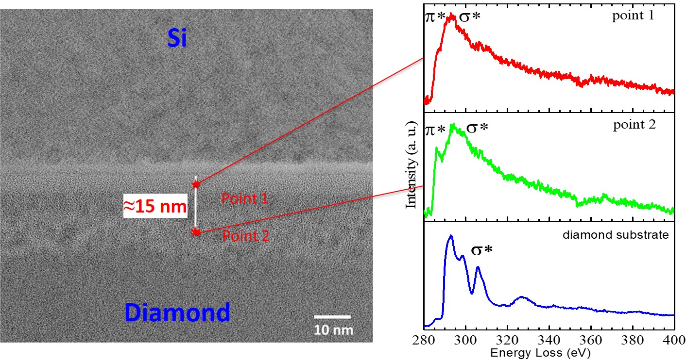 |
| A TEM image and EELS signals at diamond/Si interfaces. |
(Note) This work was jointly performed with Prof. Kasu of Saga University under the support of the Grant-in-Aid—KAKENHI—for Challenging Exploratory Research (16K13676).